What is Ion Implantation? - An Overview
In the intricate world of semiconductor manufacturing, a transformative process has quietly evolved, shaping the technological landscape for nearly three decades. Ion implantation, known as low-temperature material surface modification, represents a sophisticated interplay of science and engineering. The process accelerates ions into a solid target, causing small changes in the material's physical, chemical, or electrical properties. Tough materials like TZM, molybdenum, and tungsten are crucial, performing well in challenging environments.
A Technological Marvel with Broad Applications
The significance of the ion implantation marvel extends far beyond its niche applications. It is widely used in many industries, serving purposes from enhancing metals to ceramics and polymers. This broad use not only fuels technological progress but also brings significant economic and social gains. The process of modifying material surfaces at low temperatures is important for high technology to meet industry needs.
Microelectronics Craftsmanship: A Central Role
Within the domain of microelectronics, this discreet technique assumes a pivotal role in the craft of semiconductor fabrication. Controlling the voltage of MOSFETs is important for integrated circuits in electronics. Ion implantation's precision meets the demands of microelectronics, enabling the creation of detailed circuitry that powers our daily electronic devices.
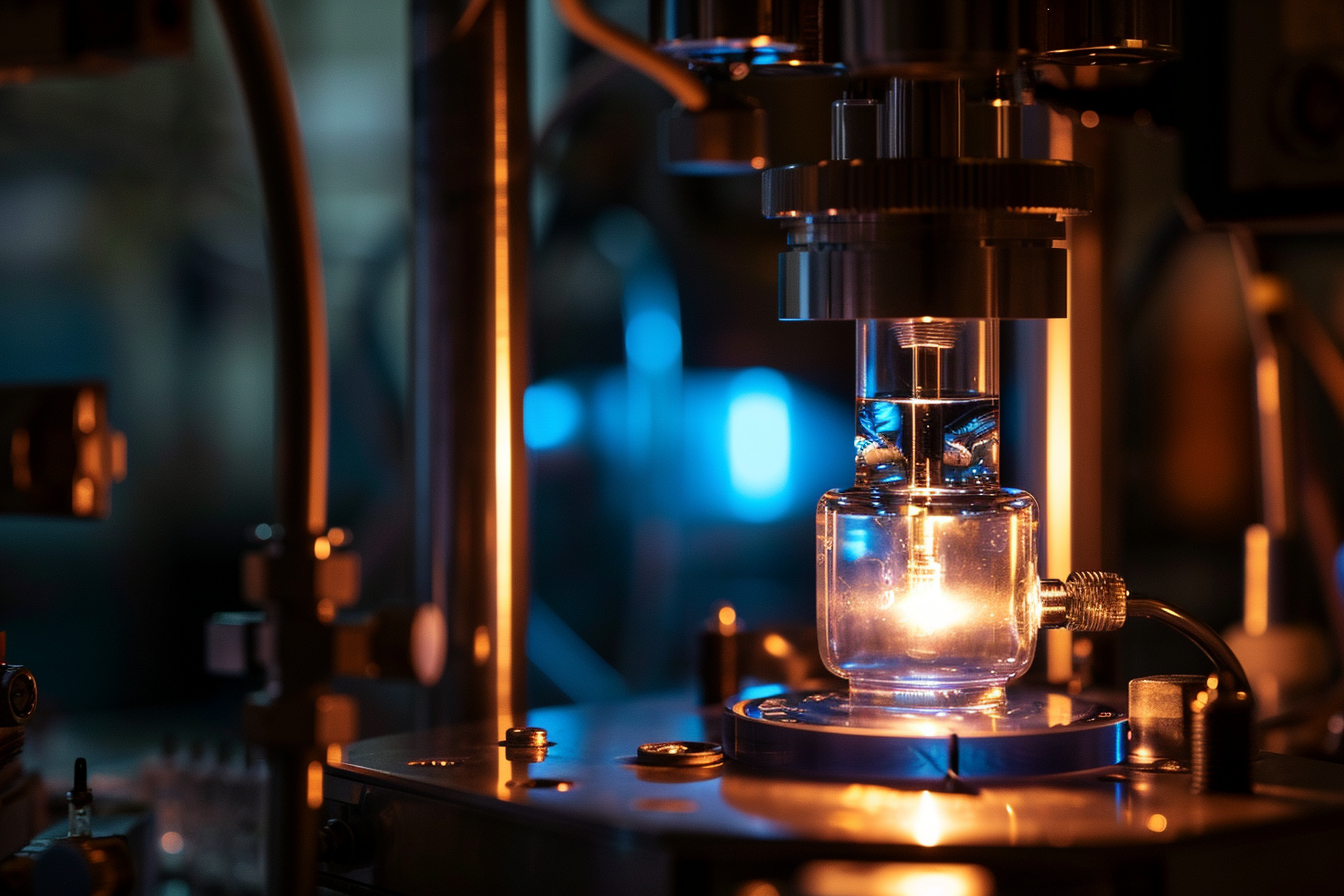
Orchestrated Precision: The Ion Implantation Process
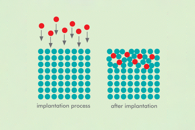
The ion implantation process unfolds in a meticulously orchestrated dance of vacuum and low temperatures. Impurity ions, charged with kinetic energy, traverse the vacuum to embed themselves directly into the semiconductor. At the same time, the process creates defects in the semiconductor structure.
To fix these issues, treatments like low-temperature annealing or laser annealing are necessary. As we move towards smaller, better electronic devices, this material modification process is leading technological progress.
The Prowess of Precision and Control
This process is impressive because it can accurately and effectively modify materials with precision and control. It navigates the helm of total impurity dose, depth distribution, and surface uniformity with a finesse that has revolutionized semiconductor manufacturing. The low-temperature nature of this methodology serves as a strategic advantage, skillfully sidestepping the pitfalls associated with original impurities and diffusion. This feature helps make perfect semiconductor structures that are crucial for electronic devices to work smoothly.
Towards a Future of Technological Evolution
As we move into a future with smaller, more efficient, and high-performance electronic devices, this simple material modification process is leading the way in technological progress. Its applications, intricately woven into the tapestry of contemporary manufacturing technologies, continue to shape the trajectory of semiconductor innovation. The potential of this transformative process remains boundless, silently propelling the semiconductor industry into new frontiers of precision and efficiency.
Expanding Horizons: Future Innovations and Challenges
While applauding ion implantation's successes, it's crucial to look forward to innovation and recognize the upcoming challenges. Researchers and engineers continually strive to enhance ion implantation technology. The quest involves refining ion sources, optimizing beamline designs, and developing advanced implantation strategies to further improve precision and efficiency.
One avenue of exploration involves the customization of ion beams to accommodate specific material properties and device requirements. Tailoring ion beams with diverse characteristics, such as energy, mass, and dose, enables finer control over the doping process. This customization is pivotal in addressing the intricate demands of emerging technologies, including quantum computing and advanced sensor applications.
Moreover, the integration of artificial intelligence (AI) and machine learning (ML) into ion implantation processes is gaining traction. These technologies offer the potential to optimize implantation parameters in real-time, adapting to variations in material composition and structure. The collaboration of AI/ML algorithms with ion implantation improves precision and allows for automated manufacturing, reducing human involvement and errors.
However, with every stride toward innovation, challenges emerge. Ion implantation-induced lattice damage remains a focal point of research. Despite advancements in post-implantation treatments, minimizing lattice defects without compromising efficiency is a delicate balance. Researchers delve into novel annealing techniques, exploring laser-based and rapid thermal annealing methods to achieve optimal results.
The scalability of ion implantation processes is another facet under scrutiny. As manufacturing scales to accommodate larger substrates and higher volumes, the efficiency and throughput of ion implantation must evolve. Engineers explore novel approaches, including parallel processing and innovative beamline architectures, to meet the demands of mass production without compromising precision.
Global Impact: Economic and Social Implications
Beyond labs and cleanrooms, ion implantation's impact reaches globally, shaping economies and societal progress. The economic implications are profound, with industries relying on ion-implanted materials experiencing increased productivity, reduced production costs, and improved product performance.
The semiconductor industry, in particular, stands as a beacon of economic growth propelled by ion implantation. The production of cutting-edge microprocessors, memory devices, and integrated circuits relies heavily on the precision afforded by ion implantation. As consumer electronics continue to evolve, the demand for advanced semiconductor devices grows, further driving the economic engine of innovation.
Moreover, the societal implications of ion implantation extend beyond the immediate economic sphere. The proliferation of electronic devices, powered by semiconductors crafted through ion implantation, has redefined communication, healthcare, transportation, and entertainment. Smartphones, improvements in medical care, and efficient transportation systems all benefit from the precision and control provided by ion implantation.
In a broader context, the environmental impact of ion implantation technology also merits consideration. The low-temperature nature of the process, compared to high-temperature alternatives, contributes to energy savings and reduced environmental footprint. As industries increasingly prioritize sustainability, ion implantation aligns with the ethos of eco-friendly manufacturing practices.
The Road Ahead: Ion Implantation in Emerging Technologies
As technology evolves, ion implantation finds itself at the forefront of enabling innovations in emerging fields. Quantum computing, a paradigm-shifting approach to information processing, relies on precisely engineered semiconductor materials. Ion implantation emerges as a key player in tailoring these materials to meet the demanding requirements of quantum bits or qubits. The ability to control and manipulate individual atoms with unprecedented precision positions ion implantation as an enabler of quantum computing breakthroughs.
Similarly, the growing area of advanced sensors and Internet of Things (IoT) devices relies on ion-implanted materials for better performance. From sensors monitoring environmental parameters to biomedical devices advancing healthcare diagnostics, ion implantation contributes to the development of highly sensitive and efficient sensor technologies.
Ethical Considerations and Responsible Innovation
Amid the technological strides, it is imperative to address ethical considerations associated with ion implantation and semiconductor manufacturing. The extraction and processing of raw materials, energy-intensive manufacturing processes, and handling of electronic waste present challenges that need ethical examination.
Responsible innovation in ion implantation involves adopting sustainable practices, optimizing resource utilization, and promoting recycling initiatives. Industry stakeholders are increasingly embracing environmentally conscious approaches, striving to minimize the ecological impact of semiconductor manufacturing. By aligning technological progress with ethical considerations, the semiconductor industry can contribute to a sustainable and responsible future.
Conclusion: The Ongoing Saga of Ion Implantation
In conclusion, the saga of ion implantation unfolds as a multifaceted narrative, intertwining scientific ingenuity, technological prowess, economic impact, and societal transformation. Starting as a basic low-temperature material surface modification, ion implantation has grown into a crucial element in semiconductor manufacturing, guiding technological progress.
The precision and control afforded by ion implantation reverberate across industries, from microelectronics to quantum computing, from advanced sensors to sustainable manufacturing practices. As we explore new technology, ion implantation shows our cleverness and helps shape the future.
The journey continues, with researchers, engineers, and industry leaders pushing the boundaries of ion implantation technology. We will solve challenges with new ideas, and follow ethical guidelines, and the global impact will influence the future of ion implantation.
Ion implantation is a special process that helps us move forward and meet our technology needs. It also guides us towards a future focused on accuracy, effectiveness, and accountability. As we explore ion implantation, its story unfolds through each implanted ion, innovation, and worldwide impact.
For more information, please visit our homepage.