2D Materials: Rising Star for Future
Introduction
2D materials, or single-layer materials, are materials with single layers of atoms. In a more micro view, 2D materials are materials at the nanoscale. The most famous 2D material example is graphene, which is consisted of carbon allotropes in a hexagonal lattice nanostructure and was first isolated in 2004. Figure 1 shows the structure of a graphene layer.
Monolayer graphene gives itself some unique properties. It has hundreds of times higher tensile strength than most steels by weight. It also has the highest thermal and electrical conductivity. Due to graphene’s superb properties, lots of studies and researchers put attention to developing other additional single-atom carbon networks such as graphdiyne, graphenylene, and others. Graphene becomes the pioneer in the development of 2D materials.
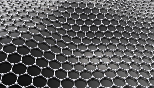
Figure 1: Graphene Layer
What Is 2D Material?
If we think about materials in three dimensions, 2D materials are materials that have only one nanosized dimension. If materials have all three dimensions in nanosized, they are 0D materials. Table 1 gives you a summary of 0 to 3D materials [1].
Table 1: 0 to 3D materials with examples
|
Number of nanosized dimensions |
Classification |
Example |
|
3 |
0D |
Quantum dots |
|
2 |
1D |
Nanotubes, nanowires, nanoribbons |
|
1 |
2D |
Single atom thick materials such as Graphene |
|
0 |
3D (Bulk) |
General materials that you can see. |
2D materials are divided into elements, metallic compounds, organics, and salts. Figure 2 shows you the structures and classifications of different 2D materials [2].
Hexagonal boron nitride (h-BN) is an isomorph of graphene (has the same microstructures as graphene which shows in Figure 1, except carbon is replaced by boron and nitride).
MoS2 is one of Transition Metal Dichalcogenides (TMDCs). The chemical formula of TMDCs is MX2 (M is the transition metal such as Mn; X is the chalcogen such as S, Se, and Te). TMDCs form X-M-X tri-layer covalent bonding structures.
Due to their different mechanical, electrical, and optical properties, 2D materials are widely used in different areas which will talk about later. Let’s first get some information about how 2D materials are produced.
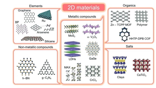
Figure 2: sorts and structures for different 2D materials [2]
How to Make 2D Materials?
2D materials are materials with single layers of atoms. It is possible to make bulk materials thinner just like cutting hams, but the problem is not so easy because of the chemical bonds of some materials in 3 dimensions. Breaking these bonds makes the thin layers very unstable and chemically reactive. Graphite is different. As a two-dimensional material, it only has strong chemical bonds within the planes, each plane overlaps together to form graphite (see Figure 3 [3]). Therefore, the strategy above can be used to make graphene.
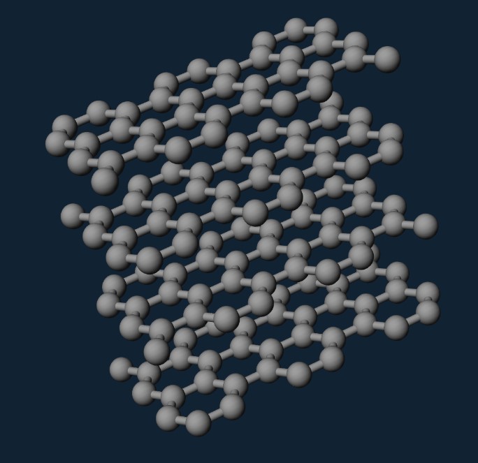
Figure 3: Graphite structure [3]
There are two ideas to make 2D materials: top-down and bottom-up.
Top-down cuts large or bulk materials under a controlled process and remove the produced layers. Its basic strategy is mentioned above. Top-down can be divided into mechanical, liquid-phase, ultrasonic, electrochemical, ion-change, and lithium-intercalated exfoliations [2].
Bottom-down uses atomic or molecular elements and “combines” them together to form 2D materials. Bottom-down uses materials smaller than 2D materials to produce 2D materials just like building blocks. Among bottom-down, there are epitaxial growth, chemical vapor deposition (CVD), pulsed laser deposition (PLD), wet chemical methods, rowaveassisted method, or topochemical transformation [2].
Mechanical exfoliation, liquid exfoliation, and CVD are commonly used to make 2D materials.
Mechanical Exfoliation
Mechanical exfoliation uses a mechanical force to separate a thin layer or a few thin layers of material from a bulk material. Usually, a piece of “sticky tape” is used to peel off the bulk material and collect the thin layers. For all top-down methods, the main important problem is to overcome the Van der Waals forces between each layer in the bulk material. By carefully applying normal force and lateral force during the peeling process, we can still produce high-quality 2D materials by mechanical exfoliation. But low efficiency and yield are the main problems for mechanical exfoliation.
Liquid Exfoliation
Liquid exfoliation can cover these disadvantages of mechanical exfoliation by using an organic solvent as an intermedium to transport mechanical force to the bulk material and sonication gives tensile stress to each layer, which separates each layer. However, 2D materials produced by liquid exfoliation may have organic solvent residuals, which makes 2D materials not suitable for some optical applications.
Chemical Vapor Deposition
Chemical Vapor Deposition (CVD) can produce high-quality and high-efficient 2D materials under controlled sizes. Within a heated furnace, one or several precursor gases that contain atomic or molecular elements hit a substrate and 2D materials will grow on the substrate. CVD is successfully applied to produce graphene and TMDCs. Gas pressures, temperature, reaction time, etc. play important roles in the quality, thickness, and composition of 2D material.
Why use 2D Material and its Application
Advantages of 2D Material
Compared with bulk material, 2D material doesn’t have Van der Waals forces because of its single-layer structure. Van der Waals forces are distance-dependent interactions between atoms or molecules. If the material cannot overcome the van der Waals forces when stressed, it will break.. Covalent bond shares electrons together which means holding the surface area-to-volume ratio ng the atoms strongly. 2D materials have no van der Waals forces but only covalent bonds,, thus exhibiting extremely strong tensile strength. Graphene is the material that has the highest tensile strength in nature.
The single-layer structure of 2D material gives it a relatively high surface area-to-volume ratio. It can contact more reactants to make faster reactions. 2D material also shows good electronic and optical properties because the reduction of periodicity in the direction perpendicular to the plane changes the band structure.
Applications of 2D Materials
2D materials are widely used in transistors, photodetectors, semiconductors, capacitors, memristors, and many other applications.
Graphene Oxide is often used to make composites of fibers, films, or 3D structures due to its supreme dispersibility. By combing 50% graphene oxide with 50% cellulose nanofibril (CNF), prepared aerogel shows stronger strength and stiffness than pure CNF aerogel [2].
Graphene’s high surface area-to-volume ratio reduces the flammability of gases [2]. This makes graphene an additive to increase the flammability resistance of polymeric composites and other materials. Graphene also shows good performance in memristors because of its high electrical conductivity, chemical stability, and high carrier mobility. It takes good responsibility in resistive switching under high speed and long-duration conditions. TMDCs, BN, or BP can also be used in memristors.
TMDCs (MoS2, WSe2, WS2) are widely used in field-effect transistors (FETs), which are the most important elements in electronics. TMDCs’ good charge mobility and moderate band gaps make them suitable for FET applications [2].
The supreme dielectric properties of h-BN film allow the combination of h-BN/Ge/metal appears in capacitors.
There are lots of applications and 2D materials that are not mentioned. Stanford Advanced Materials (SAM) provides different kinds of 2D materials. If you want more information about 2D materials, you can provide your application information to our technical staff for advice.
Reference
- 2D materials: An introduction to two-dimensional materials. Ossila. (n.d.). Retrieved January 28, 2023, from https://www.ossila.com/en-us/pages/introduction-2d-materials
- Shanmugam, V., Mensah, R. A., Babu, K., Gawusu, S., Chanda, A., Tu, Y., Neisiany, R. E., Försth, M., Sas, G., & Das, O. (n.d.). A review of the synthesis, properties, and applications of 2D materials. A Review of the Synthesis, Properties, and Applications of 2D Materials. Retrieved January 29, 2023, from https://onlinelibrary.wiley.com/doi/full/10.1002/ppsc.202200031
- Shanmugam, V., Mensah, R. A., Babu, K., Gawusu, S., Chanda, A., Tu, Y., Neisiany, R. E., Försth, M., Sas, G., & Das, O. (n.d.). A review of the synthesis, properties, and applications of 2D materials. A Review of the Synthesis, Properties, and Applications of 2D Materials. Retrieved January 29, 2023, from https://onlinelibrary.wiley.com/doi/full/10.1002/ppsc.202200031