PRODUCT

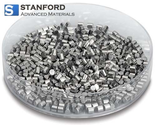
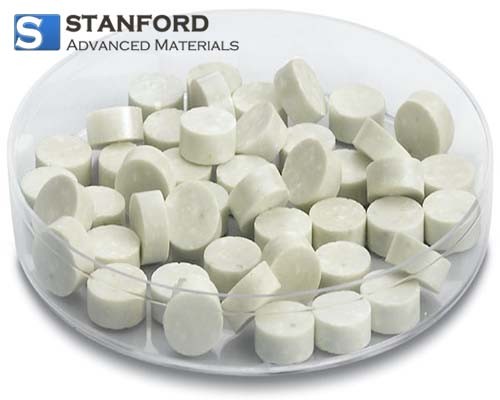
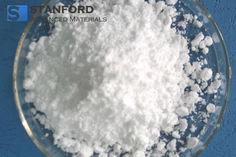
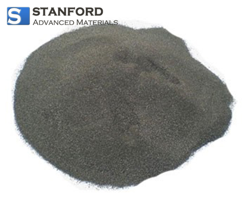
Metals
Precious Metals
Tantalum
Niobium
Molybdenum
Tungsten
Titanium
Zirconium
Rhenium
Iridium
Indium
Hafnium
Beryllium
Nickel
Aluminum
Exotic Metals
Antimony
Barium
Bismuth
Cadmium
Calcium
Cerium
Chromium
Cobalt
Copper
Dysprosium
Erbium
Europium
Gadolinium
Gallium
Germanium
Gold
Holmium
Iron
Lanthanum
Lead
Lithium
Lutetium
Magnesium
Manganese
Palladium
Platinum
Potassium
Praseodymium
Rhodium
Rubidium
Ruthenium
Samarium
Scandium
Silver
Sodium
Terbium
Thulium
Tin
Vanadium
Ytterbium
Yttrium
Zinc
INDUSTRIES
Chemical & Pharmacy
Pharmaceutical Industry
Aerospace
Agriculture
Automotive
Chemical Manufacturing
Defense
Dentistry
Electronics
Energy Storage & Batteries
Fuel Cells
Investment Grade Metals
Jewelry & Fashion
Lighting
Medical Devices
Nuclear Energy
Oil & Gas
Optics
Paper & Pulp
Pharmaceuticals & Cosmetics
Plating
Research & Laboratory
Solar Energy
Space
Steel & Alloy Producers
Sports Equipment
Textiles & Fabrics
APPLICATIONS
Tungsten Applications
Metallurgy
Semiconductor
Rare-earth Magnets
Catalyst
3D Printing Powder
High Entropy Alloy Powder
Metal Injection Molding
Additive Manufacturing
Thermal Spraying Coatings
Hot Isostatic Pressing
Rare Earth Element Application
Environmental Catalysts
Grinding Wheels
OLED Materials
Thermocouple Wire
Packing & Internals
Li-ion Battery & Electronic Chemicals
Metal Powders for Diamond Tools
Soft Magnetic Powder
-
- Chemical & Pharmacy
- Pharmaceutical Industry
- Aerospace
- Agriculture
- Automotive
- Chemical Manufacturing
- Defense
- Dentistry
- Electronics
- Energy Storage & Batteries
- Fuel Cells
- Investment Grade Metals
- Jewelry & Fashion
- Lighting
- Medical Devices
- Nuclear Energy
- Oil & Gas
- Optics
- Paper & Pulp
- Pharmaceuticals & Cosmetics
- Plating
- Research & Laboratory
- Solar Energy
- Space
- Steel & Alloy Producers
- Sports Equipment
- Textiles & Fabrics
-
- Tungsten Applications
- Metallurgy
- Semiconductor
- Rare-earth Magnets
- Catalyst
- 3D Printing Powder
- High Entropy Alloy Powder
- Metal Injection Molding
- Additive Manufacturing
- Thermal Spraying Coatings
- Hot Isostatic Pressing
- Rare Earth Element Application
- Environmental Catalysts
- Grinding Wheels
- OLED Materials
- Thermocouple Wire
- Packing & Internals
- Li-ion Battery & Electronic Chemicals
- Metal Powders for Diamond Tools
- Soft Magnetic Powder