PRODUCT
SDS

Where Do You Find Tantalum

With its high boiling point, good resistance to corrosion, low coefficient of thermal expansion, and high co-efficient of capacitance, Tantalum is a key element widely used in the electronic industries in the manufacture of sputtering targets and capacitors as well as in the medical industry for orthopedic implants.

tantalum minal

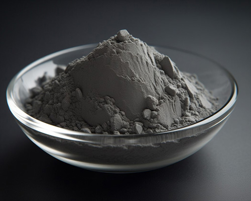
Tantalum occurs in columbium ores. As the demand for columbium increases, increasing amounts of tantalum concentrates become available. Tantalum can be made as various of shapes such as powders, ingots, foils and plates. After a difficult and complex separation and reduction process, both metals are obtained in the form of powder.

The tantalum powder is pressed in dies to form bars which are vacuum-sintered by passing high currents through them in much the same way that tungsten powder is consolidated. Ingots may then be cast in consumable-electrode vacuum-arc furnaces or electron-beam furnaces. The ingots are worked cold because of the reaction of tantalum with air at high temperatures. Heavy cold working is possible because of the high room-temperature ductility of tantalum. Intermediate annealing must be done in vacuum furnaces.

Tantalum is resistant to oxidation by air to about 500 F. It has been used as a container for molten sodium, potassium, and other metals and alloys at temperatures as high as 2200 F (in the absence of air) without being attacked.

Tantalum has exceptional resistance to most corrosive media below 300 F. For this reason, tantalum is used in many applications involving exposure to corrosive environments in the chemical industry.

About the author

Chin Trento

Chin Trento holds a bachelor’s degree in applied chemistry from the University of Illinois. His educational background gives him a broad base from which to approach many topics. He has been working with writing advanced materials for over four years in Stanford Advanced Materials (SAM). His main purpose in writing these articles is to provide a free, yet quality resource for readers. He welcomes feedback on typos, errors, or differences in opinion that readers come across.

REVIEWS
{{viewsNumber}} Thought On "{{blogTitle}}"
{{item.created_at}}

{{item.content}}

LEVE A REPLY (Cancle reply)

Your email address will not be published. Required fields are marked*

Comment
Name*
Email*
{{item.children[0].created_at}}

{{item.children[0].content}}

{{item.created_at}}

{{item.content}}

More Replies

LEAVE A REPLY

Your email address will not be published. Required fields are marked*

Comment
Name*
Email*

Related News & Articles

MORE >>
Comparing SOI vs. Silicon Wafers: What’s Best for Your Semiconductor Project?

There are significant differences between SOI and silicon wafers in terms of material structure, performance characteristics application areas, etc.

READ MORE >
An Overview of Calcium Carbonate Crystal Substrates

Calcium carbonate crystal substrates represent a burgeoning field in material science.

READ MORE >
Silicon Carbide vs. Silicon: A Comparative Study of Semiconductors in High-Temperature Applications

Compared with silicon, silicon carbide tends to have a wider range of applications in higher temperature scenarios, but due to its preparation process and the purity of the finished product obtained, silicon wafers are still the more commonly used choice in cases where the temperature environment requirements are relatively low.

READ MORE >
Leave A Message
Leave a Message
*Your Name:
*E-mail:
*Product name:
*Your Phone:
*Message: