An Overview of Ion Implantation
Introduction
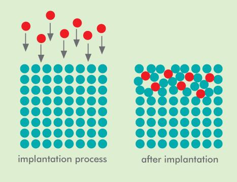
Ion implantation is the low-temperature process by which ions of one element are accelerated into a solid target, thereby changing the physical, chemical, or electrical properties of the target. The components of ion implantation are often made of TZM alloy, molybdenum, tungsten because these materials could perform well in the harsh environment.
Ion implantation is a booming and widely-used high technology of material surface modification in the world for nearly 30 years. Due to its unique and outstanding advantages, the high technology has an extremely widespread application in the doped semiconductor material, the surface modification of metal, ceramics, polymers, etc, which obtained the huge economic and social benefit.
In the electronic industry, ion implantation has become one of the important doping techniques in the microelectronic craft; also, it is an important means of controlling the MOSFET threshold voltage. So it can be said that ion implantation is a kind of indispensable means in the manufacture of the large scale integrated circuit in contemporary.
The method of ion implantation
The method of ion implantation is accelerating in a vacuum and low temperature, thus the impurity ions with kinetic energy can go directly into semiconductor; at the same time it also can produce some lattice defects in the semiconductor, these defects should be eliminated with low-temperature annealing or laser annealing after ion injection. The impurity concentration of ion implantation generally distributes as Gaussian distribution, and the highest concentration is not on the surface but within a certain depth.
The advantages of ion implantation
The advantages of ion implantation are that it can control the total dose of impurities, the distribution of depth and uniformity of surface precisely, moreover, the low-temperature process of which can avoid the original impurities and diffusion, etc. At the same time, it can realize the goal of developing the alignment technology to reduce the capacitance effect.
General principle
What is the general principle of Ion implantation? Ion implantation equipment typically consists of an ion source, where ions of the desired element are produced, an accelerator, where the ions are electrostatically accelerated to high energy, and a target chamber, where the ions impinge on a target, which is the material to be implanted. Thus ion implantation is a special case of particle radiation. Each ion is typically a single atom or molecule, and thus the actual amount of material implanted in the target is the integral over time of the ion current. This amount is called the dose. The currents supplied by implants are typically small (micro-amperes), and thus the dose which can be implanted in a reasonable amount of time is small. Therefore, ion implantation finds application in cases where the amount of chemical change required is small.
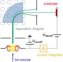
The energy of the ions, as well as the ion species and the composition of the target, determine the depth of penetration of the ions in the solid: A monoenergetic ion beam will generally have a broad depth distribution. The average penetration depth is called the range of the ions. Under typical circumstances, ion ranges will be between 10 nanometers and 1 micrometer. Thus, ion implantation is especially useful in cases where the chemical or structural change is desired to be near the surface of the target. Ions gradually lose their energy as they travel through the solid, both from occasional collisions with target atoms (which cause abrupt energy transfers) and from a mild drag from the overlap of electron orbitals, which is a continuous process. The loss of ion energy in the target is called stopping and can be simulated with the binary collision approximation method.
Industrial applications
Ion implantation technology has been applied in many fields of industrial production, among which metal material industry and semiconductor industry are widely used.
* Modification of metal material
Ion implantation applied to metal material modification is to inject the ions of certain amount and energy into the surface of metal materials which are treated by heat treatment or surface coating process to change the chemical composition, physical structure and phase state of the material surface, then the mechanical, chemical and physical properties of the materials can be changed. Specifically, ion implantation can change the acoustics, optics and superconducting properties of materials, and improve the working hardness, wear resistance, corrosion resistance and oxidation resistance of materials. At present, it has been applied to the air hydraulic pump distribution, internal combustion engine precision coupling, automobile engine parts, hard alloy cutting tools, and large size precision wear-resisting parts.
* Prolong the service life of the die
As a new surface strengthening process, ion implantation has been applied in different materials and has achieved many achievements. Due to the different working conditions, many failure forms have appeared in the mold of the same material, and the advantages of ion implantation process can make up for these defects. As long as the designer uses different ion implanted devices to inject different elements into the mold selectively according to different failure forms, the goal of extending the service life of the mold can be achieved conveniently.
* Semiconductor industry
With the development of ion implantation equipment, ion implantation technology has developed rapidly in the integrated circuit industry. Because of the good controllability and repeatability of ion implantation technology, the designer can design ideal impurity distribution according to the requirements of circuit or device parameters.
The manufacture of a complete semiconductor device in a modern semiconductor manufacturing process usually involves many steps (15 ~ 25 steps) of ion implantation. The main process parameters of ion implantation are impurity type, injecting energy and doping dosage. The types of impurities can be divided into n-type and p-type. The injection of energy determines the depth of the impurity atoms injected into the silicon, the high energy is injected deeply, and the low energy is injected lightly. Doping does refer to the concentration of impurity atoms, which determines the conductivity of the doping layer. With the progress of semiconductor technology, the process of ultra-shallow junction becomes the key, especially when making semiconductor devices under 65nm. The ion implantation process, with its precise injection depth and the controllability of the concentration, and the stable repeatability, shows its importance in the manufacture of advanced semiconductor devices again.
Stanford Advanced Materials (SAM) provides customized ion implantation components with high quality and competitive price, which includes ion implantation components (Tungsten), ion implantation components (Molybdenum), ion implantation components (TZM Alloy), etc.