The Impact of Silicon Wafer Quality on Semiconductor Performance and Reliability
1 Introduction
The semiconductor market continues to grow as the economy recovers. Emerging applications such as 5G and new energy vehicles bring a new round of growth to the global semiconductor industry. Data from the World Semiconductor Trade Statistics Organization (WSTS) shows that the global semiconductor market size in 2022 will grow by 3.3% year-on-year to reach a record high of $574 billion.
As a semiconductor chip base material, the silicon wafer industry will also enter a high-speed development. As part of the consumer electronics demand rebound and AI outbreak demand boost, the 12-inch wafer fab has been in the second half of 2023 gradual recovery. In the accelerated development of the leading enterprises and the gradual recovery of end demand, the segment will realize double-digit growth in 2024.
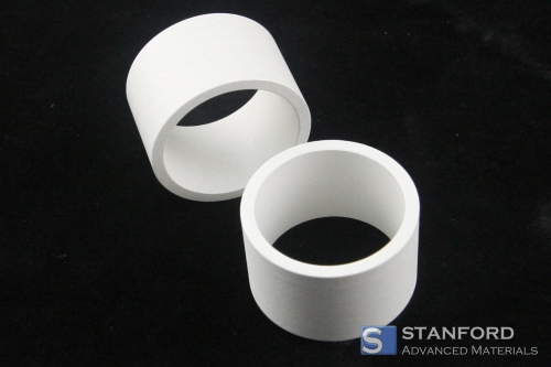
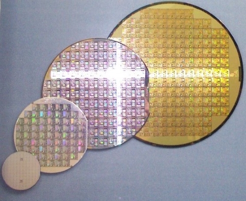
As a critical base material in semiconductor manufacturing, the crystal quality of Silicon Wafers (Fig. 1) directly affects the properties of the finished semiconductor device. The effect of lattice quality and grain boundary defects on the electron mobility of silicon wafers directly affects the speed and power consumption of the device and may increase the leakage current of the device. The flatness and degree of contamination on the surface of a silicon wafer can have a significant impact on key steps such as lithography, thin film deposition, and etching. Impurities and doping in silicon wafers can lead to increased electron trapping, shorter carrier lifetimes, and drift in device parameters. In addition, temperature and pressure stresses may be introduced during silicon wafer preparation and subsequent processing, affecting the mechanical stability and electrical properties of the crystals.
2 Key Factors Determining the Quality of Silicon Wafers
2.1 Crystal Structure: Purity of Single Crystal Silicon, Crystal Defects
The key factors determining the quality of silicon wafers in terms of crystal structure are most often mentioned as crystal purity and crystal defects.
1. Crystal purity: The purity of single-crystal silicon is critical to its electrical properties. Typical industrial silicon (99.0-99.9%) does not have semiconductor properties, but when purified to a very high purity (99.999999999%), it shows excellent semiconductor properties. High-quality monocrystalline silicon usually reaches 99.999999999% (9 of 9) or more at the electronic level.
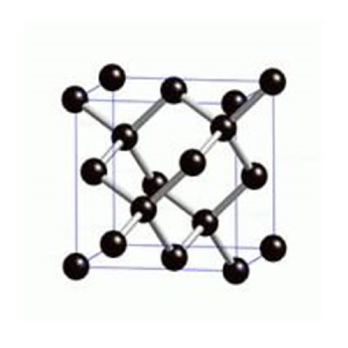
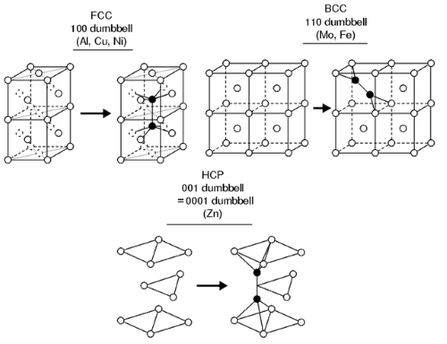
2. Crystallographic defects: The actual crystal space array and the ideal space array are different, as they cannot be made to the absolute ideal regular periodic arrangement (Fig. 2). Instead, in the arrangement, there are irregularities and aberrations, deviations from the ideal space array. Those structures or regions that deviate from the dot matrix are commonly known as crystal defects.
Among them, dislocation is a very important crystal defect. The dislocation of a crystal is a very long line around which the atoms in a certain range are regularly misaligned, leaving its original equilibrium position, so it is called dislocation.
2.2 Surface Quality: Flatness, Roughness, Particle Contamination
1. Surface contamination: This defect refers to foreign matter such as dust, particles, and pollutants attached to the surface of the wafer, which comes from the debris generated in the processes of cutting, polishing, cleaning, etching, etc., or the dust in the air, or the residue of chemical reagents. These redundancies affect the flatness and cleanliness of the wafer, as well as the quality of the subsequent lithography, doping, and other processes, which can lead to defects in the structure of the integrated circuit or changes in the electrical characteristics of the chip.
2. Mechanical damage: This defect refers to the wafer surface or edge of the scratches, chipping, peeling, and other phenomena, in the wafer cutting, polishing, handling, and other processes generated by the impact or friction, or the quality of the blade or the parameters of the inappropriate may lead to a reduction in surface flatness. These mechanical damages affect the integrity and stability of the wafer and may lead to breakage or detachment of the chip.
2.3 Dimensional Accuracy: Wafer Diameter, Thickness, Warpage
The size and thickness of wafers are not chosen arbitrarily but are based on process requirements and physical properties. When the wafer size becomes larger, the thickness of the wafer is increased accordingly to maintain its mechanical strength and warpage while avoiding damage due to stress or bending during processing. Wafers are subjected to various physical and chemical treatments in the manufacturing process, including etching, ion implantation, oxidation, diffusion, etc. These processes may cause the wafer to be subjected to mechanical stress, and if the wafer is too thin, it may fracture or break. Wafers need to be handled and positioned during processing. If the wafer is too thin, it may be bent, affecting processing accuracy.
3 How Silicon Wafer Quality Factors Affect Semiconductor Device Performance
3.1 Crystal Structure, Lattice Defects
The more common dislocations in lattice defects have a significant impact on the electrical properties of silicon single crystals. For example, dislocations affect resistivity, and carrier concentration, shorten the lifetime of minority carriers, and reduce electron mobility.
1. Resistivity effect: Dislocations introduce localized stress fields and non-uniformities within the crystal, leading to increased scattering of electrons and holes. This scattering leads to blocked carrier migration, which increases the material's resistivity.
2. Carrier concentration effects: Dislocations can introduce additional impurity atoms or change the arrangement of atoms in the lattice, thus changing the carrier concentration of the semiconductor material. For example, a localized stress field near a dislocation may cause the position of atoms to be shifted or deformed, which in turn affects the generation and suppression of carriers.
3. Shortened minority carrier lifetime: Dislocations increase the carrier complexity in the material. In semiconductors, carrier complexation leads to shortened lifetimes of minority carriers (e.g., electrons or holes within the diffusion length of the minority carriers). The localized stress field and non-uniformity introduced by dislocations can increase carrier interaction and promote the compounding process.
4. Reduced electron mobility: Dislocations cause distortions and non-uniformities in the crystal lattice, which can lead to impeded movement of carriers within the crystal. Especially for electrons, are scattered in the lattice by defects such as dislocations and grain boundaries, which reduces the electron mobility.
3.2 Surface Flatness
The surface flatness of a silicon wafer has a cascading effect on semiconductor devices. It not only directly affects the quality of the contact surface in contact with other materials or devices, such as metal electrodes and packaging materials. The quality of the contact surface directly affects the value of the contact resistance, and an uneven contact surface under the influence of external forces to produce various data changes will also have an impact on the performance and reliability of the device.
In addition, the flatness of the surface of the silicon wafer and contamination and other surface conditions will also affect the use of photolithography, and etching technology to define the structure. Etching technology and photolithography are often used in the semiconductor device manufacturing process of engraving the structure and pattern of the device, the surface condition of the silicon wafer directly affects the accuracy of photolithography and etching, the quality and uniformity of the graphics and the shape and size of the device produced by the decisive role.
Silicon wafers as an important thin film deposition substrate material, their surface flatness directly affects the quality of the film deposited on the surface. Defects and contamination on the surface of silicon wafers can lead to uneven film deposition, film thickness inconsistencies, bubbles, cracks, and other defects, thus affecting the performance and stability of the device.
3.3 Grain Boundaries and Impurities
The resistivity of a semiconductor is very sensitive to the amount of impurities it contains. Even tiny impurities can seriously affect the electrical properties of silicon, such as conductivity and carrier mobility. In particular, some impurities such as iron, copper, and magnesium have a large impact on the electrical properties. The presence of impurities may lead to electron scattering and local non-uniformity in the crystal, thus reducing the performance and reliability of the device. Changes in impurity content can cause significant changes in the resistivity of semiconductor materials. For example, when the concentration of phosphorus impurities in silicon varies within the range of 1021-1012 cm-3, its resistivity changes from 10-4 Ω.cm to 104 Ω.cm. There are not many materials whose resistivity can vary over such a wide range, which illustrates that the impurity content of semiconductors is one of the main factors in determining their resistivity.
3.4 Wafer Size, Thickness, Warpage
In the manufacturing process, the larger the diameter of the silicon wafer size is undoubtedly more favorable to the manufacturer. In the large size and large diameter silicon wafers can produce more chip devices, equipment production efficiency can be effectively improved; at the same time the edge of the wasted material will be reduced to reduce additional costs; in addition to improving the equipment reuse rate.
But the size of the silicon wafer is not an arbitrary decision, it depends on the processing capacity of the production equipment, because the material itself the role of stress, when the wafer size increases, its thickness will need to be increased accordingly, to maintain the structural stability of the material, otherwise the size of the large, thin thickness of the wafer material warping will be a corresponding increase in the thickness of the wafer material will even appear fracture loss and other phenomena.
4 How Silicon Wafer Quality Affects Semiconductor Reliability
4.1 Effect of Defect Density on Device Lifetime
The life of a semiconductor device is determined primarily by its physical life and maintenance life. Physical life refers to the time when a semiconductor device fails due to material aging or wear and tear under normal operating conditions. Defects in silicon wafers may accelerate the aging process of the material, causing the device to fail in a shorter period. At the same time, defects may also lead to current leakage, reduced thermal stability, and other problems, further affecting the life of the device.
Repair life is the time that a semiconductor device can be repaired and continues to operate normally after a failure. However, if the defect density of silicon wafers is too high, it may make it difficult to restore the original performance of the device during the repair process or make the repair cost too high, thus reducing its repair life.
Defects in silicon wafers also affect the reliability of semiconductor devices. Defects in the crystal structure cause particles to be cheap from the ideal position of the crystal structure, thus leading to bonding in different positions and changes in the crystal structure, which is manifested as uneven stress, which may lead to instability or sudden failure of the device during operation, thus affecting the stability of the entire electronic system.
4.2 Relationship of Wafer Quality to Leakage Current and Breakdown Voltage
Leakage current is the current that should not flow in a semiconductor device under normal operating voltage. When there are defects in a silicon wafer, such as impurities, lattice distortions, microcracks, etc., these defects, as well as impurities, especially impurity particles with conductive properties, may form conductive channels that cause current to flow where it should not, thereby generating leakage current. The presence of leakage current not only increases the power consumption of the device but may also cause the temperature of the device to rise, further affecting the performance and life of the device.
Breakdown voltage is the maximum voltage that a semiconductor device can withstand under normal operating conditions. Beyond this voltage, the device may experience a breakdown, which is a sudden increase in current, resulting in damage to the device. Defects in silicon wafers may reduce the breakdown voltage of a device because there may be a concentration of electric fields or structural fragility at the defects, allowing the device to break down at lower voltages. Thus, the quality of the silicon wafer has a significant effect on the breakdown voltage.
5 Silicon Wafer Fabrication and Quality Control
5.1 Crystal Growth Technology for Silicon Wafers
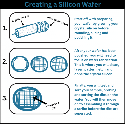
The Lift-off method is now commonly used to grow silicon crystals. The crucible is filled with silicon and heated so that the temperature in the crucible is maintained at 1685°C. This temperature is about 100°C above the melting point of silicon alone, so the silicon alone in the crucible is in a molten state. In the upper part of the crucible, there is a lifting rod, and there is a mechanical device to make the lifting rod lift and rotate freely. A small piece of monocrystalline silicon is immersed into the crucible by fixing it at the top of the lever. This single crystal of silicon acts as a "seed" and attracts the surrounding silicon atoms to arrange themselves around it to form a crystal. The crystal grows as it is slowly pulled and rotated, and the parts that are pulled out all belong to the same single crystal. The large single crystal is 200 millimeters in diameter, which is thicker than your arm. Such a crystal has no interface, no defects, and can be said to be the most perfect single crystal that human beings can make. To ensure the purity of the material and avoid non-uniform nucleation, all operations should be carried out under vacuum or inert gas protection. To prevent dislocations from occurring in the crystal, the traditional single-crystal silicon lifting method is to make a thin neck at the beginning of the crystallization growth, which is called the "necking method". Due to the strength of the necking, it is difficult to lift monocrystalline silicon weighing more than 100 kilograms. Scientists in the seed crystal after adding a considerable amount of boron, greatly enhanced the strength of the seed crystal, preventing the dislocation of the crystal, and therefore no longer need to produce a 3 mm diameter neck. This new method will replace the use of 30 years of necking method, it is not only able to produce large single crystal silicon but also able to shorten the crystal growth time and improve yield, for the cheap production of ultra-large-scale integrated circuits needed to provide the possibility of large single crystal silicon.
Wafer growth requires polysilicon into the furnace quartz crucible, vacuum, or pass inert gas after melting. After the molten silicon is stabilized, single crystals can be pulled, and a piece of seed crystal that has already determined the internal crystal direction is used as a guide on the liquid surface. By controlling the height of the crucible liquid surface, the temperature of the solid-liquid interface, and the speed of rotation of the seed crystal, the silicon is transformed from a liquid again into a solid with a uniform internal crystalline direction to grow large-diameter single crystals. The automatic adjustment process and the lifting speed are controlled by computers, which guarantees the isotropic growth of monocrystalline silicon.
5.2 Surface Treatment Technology for Silicon Wafers
After cutting the wafers need to go through the surface treatment to ensure the flatness of the wafer surface as well as free from impurity contamination. The more widely used treatment methods are photolithography, etching, etc. There are also some cleaning techniques such as plasma cleaning, which can not only clean the surface of the wafer but also improve the surface activity, improve the bonding ability of the material surface, improve the welding ability, hydrophilicity, and so on.
In addition, there are some innovative treatment methods such as placing the wafer in a reaction chamber with a reaction gas; reacting the reaction gas with the oxides on the surface of the wafer to form a reaction product; and annealing the wafer at least twice to decompose and remove the reaction product. The surface treatment method enables the reaction products generated in the surface treatment process to be decomposed multiple times by annealing the wafer multiple times, and each annealing treatment decomposes the reaction products so that the thickness of the reaction products continues to decrease, and at the same time reduces the difficulty of decomposition of the reaction products due to the thickness of the reaction products being too thick, and then makes it easier to decompose the reaction products on the surface of the wafer, and reduces the number of times the wafer is annealed during the surface treatment process, and reduces the number of times the surface treatment method is annealed. This reduces the amount of reaction product residue on the wafer surface during the surface treatment process.
5.3 Inspection Techniques for Silicon Wafer Quality
Due to the presence of wafer defects, chip failures can occur during functional integrity testing of all chips on a wafer. Chip engineers mark the test results with different colors to distinguish the location of the chips. Under the influence of different operating processes, specific spatial patterns are generated on the wafer accordingly. Hansen et al. in 1997 pointed out that defective chips usually have aggregation phenomena or exhibit some systematic patterns, and such defective patterns usually contain necessary information about the process conditions. The wafer map not only reflects the integrity of the chip but also accurately describes the spatial location information corresponding to the defect data. The wafer map may show spatial dependence across the entire wafer, and chip engineers can often trace the cause of defects and solve problems based on the type of defect. For wafer patterns with large areas, small feature sizes, low densities, and low integration, the lithography paths can be observed with an electron microscope, and trace detection can be performed directly. An image signal processing system can also be used for detection, where the image signal is decomposed into different frequency subbands by filters, and then the average, standard deviation and other statistics such as wavelet coefficients are detected and calculated to detect anomalies.
6 Conclusion
As a fundamental material in semiconductor manufacturing, the crystal quality of silicon wafers directly affects the properties of finished semiconductor devices. Technological advances in production and testing processes have led to a gradual improvement in the purity and precision of silicon wafers, which will be used in a wider range of applications and more accurate materials in the future. For a better application experience, Stanford Advanced Materials will not only provide high-quality silicon wafer products but also provide you with complete services, including consultation and after-sales processing.
Related reading:
Gallium Arsenide Wafer VS. Silicon Wafer
Graphene Growth and Adherence to Silicon Wafers
References:
[1]Masataka H ,Daiki T ,Oga N , et al. Experimental study on the effect of impurity concentration on phonon and electronic transport properties of single-crystal silicon[J]. Results in Physics,2023,47.
[2]Martin M ,P. P M ,Yi S B , et al. Effect of grain boundary scattering on carrier mobility and thermoelectric properties of tellurium incorporated copper iodide thin films[J]. Surfaces and Interfaces,2023,41.