The Ultimate Guide to Crystal Materials
Crystals can realize the interaction and conversion of electricity, magnetism, light, sound and force, etc. It is an indispensable and important material in the development of modern science and technology.
Especially due to the rapid development of solid-state microelectronics, there is a greater need for a large variety of crystal materials, including semiconductor crystals, laser crystals, scintillation crystals, optical crystals, superhard crystals, insulating crystals piezoelectric crystals, etc. Crystal materials are at the forefront of the development of materials science, which are closely related to new technologies such as space, electronics, laser, new energy development and biomedicine. The types of crystal materials and their applications are extremely wide.
In this paper, we will briefly introduce some common crystal materials and their applications.
Semiconductor Crystals
Semiconductor crystals are the main basic material for the semiconductor industry. It occupies the top position among crystal materials in terms of its wide application and importance.
Semiconductor crystal is developed in the 1950s, the first generation of semiconductor representative materials: germanium (Ge) single crystal and silicon single crystal (Si), made from them a variety of diodes, transistors, field-effect tubes, silicon controllers and high-power tubes and other devices, so that the integrated circuit from only a dozen units of circuit rapid development to contain thousands of components of the ultra-large-scale integrated circuit, triggered the integrated circuit ( IC) as the core of the rapid development of the field of microelectronics, greatly improving the reliability of the work of integrated circuits while reducing costs. In turn, it has promoted the wide application of ICs in space research, nuclear weapons, missiles, radar, electronic computers, military communication equipment and civil applications.
The second generation semiconductor materials are compound semiconductors mainly gallium arsenide (GaAs), indium antimonide (InSb) and indium phosphide (InP), which are mainly used to make high-frequency, high-speed and high-power electronic devices, and are widely used in the fields of satellite communications, mobile communications and optical communications. GaAs, InP and other compound materials are scarce, need to be formed by synthesis, the price is relatively high, and more harmful to the environment, making it difficult to be more widely used and more limited, and gradually replaced by the third generation of semiconductor materials.
The third generation semiconductor materials are mainly wide band semiconductor materials represented by silicon carbide (SiC), gallium nitride (GaN), zinc oxide (ZnO), diamond, and aluminum nitride (AlN). Compared with the first generation and second generation semiconductor materials, the third generation semiconductor materials have wide band width, high breakdown electric field, high thermal conductivity, high electron saturation rate and higher radiation resistance, and thus are more suitable for making high temperature, high frequency, radiation resistance and high power devices, and are usually called wide band semiconductor materials (band width greater than 2.2ev), also known as high temperature semiconductor materials.
Optical Crystals
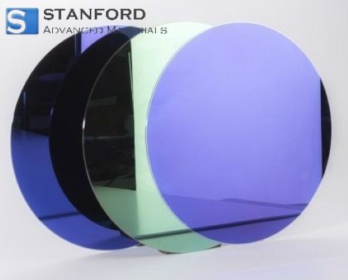
Optical crystals are used as optical components of crystals, such as lithium halide crystal fluoride, calcium fluoride, magnesium fluoride, barium fluoride, they have good transmission characteristics in the ultraviolet and infrared, so they can be used as ultraviolet excimer laser and some infrared laser output window, lens, prism, rotor, wave sheet, etc.; oxides such as sapphire Al2O3, yttrium vanadate YVO4, crystal, etc. can also be used as the work of the above lasers Oxide such as sapphire Al2O3, yttrium vanadate YVO4, crystal, etc. can also be used as output window, lens, prism, etc. of the above lasers.
Laser crystal
Laser is a wonderful "substance", is another great discovery of mankind after the atomic energy, computers and semiconductors. As we all know, the brightness of laser is so high that it can reach one billion times the brightness of the sun or even higher; the laser is pure and monochromatic; the laser has incomparable collimation (straight line propagation); and, the laser has powerful energy, and the instantaneous burst of energy can penetrate and melt even the hardest objects. Therefore, lasers are widely used in production, life and research, and are a powerful tool for people to explore nature.
The device that generates laser light is called a laser. Among the various lasers currently available, all-solid-state lasers are the most promising ones. Laser crystal (lasercrystal), a crystal material that converts the energy provided by the outside world into a highly parallel and monochromatic laser that is coherent in space and time through an optically resonant cavity, is the working substance of crystal lasers and is the basic support material for solid-state laser technology and industry. Common laser crystal materials include Nd:YAG, Nd:YVO4, Nd:YLF, titanium gem crystal, ruby crystal, etc.
Scintillation crystal
Under the impact of high-energy particles, the crystal that can change the kinetic energy of high-energy particles into light energy and emit fluorescence is called scintillation crystal. Scintillation crystal can be used for the detection of x-ray, γ-ray, neutron and other high-energy particles. The detection and imaging technology with scintillation crystal as the core has been widely used in nuclear medicine, high-energy physics, security inspection, industrial nondestructive flaw detection, space physics and nuclear prospecting, etc. Usually applied scintillation crystal materials are cultivated by artificial methods, and there are many kinds. Currently, the more used scintillation crystals are BGO (abbreviation of the general name of the Bi2O3-GeO2 system compound bismuth germanate), CsI (cesium iodide), PbWO4 (lead tungstate), etc.
Super hard crystals
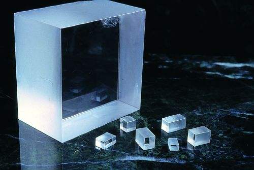
Diamond, also called "diamond", is a natural mineral and the hardest material in nature. It is a single crystal composed of carbon elements formed under high pressure and high temperature in the deep part of the earth over a long period of time. Diamonds that can be found and mined in nature are extremely rare, usually only a total of 1 carat of finely crushed diamonds can be obtained per 4 cubic meters of rich ore, and large size diamonds that are crystal clear and flawless are even rarer.
Since the 1950s, people have researched and developed a variety of methods to synthesize diamond artificially, mainly high temperature and high pressure (HTHP), chemical vapor deposition (CVD), blast method, etc. In 1955, GE used HTHP to synthesize diamond crystals for the first time. In the 1980s, the world launched a research boom on CVD diamond, and various preparation methods such as hot filament method (HFCVD), microwave plasma (MPCVD) and DC arc plasma jet CVD were developed, which laid the foundation for the later applications.
The high hardness is one of the many characteristics of diamond. Using the extremely high hardness of diamond, it can be prepared into various tools, which play an irreplaceable role in processing stone, non-ferrous metals, difficult to machine composite materials (such as carbon fiber composites), etc., and can achieve efficient, high-precision and environmentally friendly processing.
In the process of using diamond in large quantities, people have also observed its shortcomings. One of the most prominent point is that, when processing some hard materials with diamond, such as grinding a large number of steel and sintered silicon carbide, the surface temperature of diamond up to 1500 ~ 2000 ℃, in this condition, the strength of diamond rapidly decreases, and very easy with the oxygen in the air antagonistic to produce similar "burning" phenomenon. At the same time, the diamond itself is continuously reduced to soft graphite which is useless for grinding, thus leading to a very rapid loss the of diamond. After people's continuous exploration, a new type of superhard material cubic boron nitride crystal was synthesized to make up for the disadvantage of diamond, cubic structure of boron nitride - CBN, its crystal structure is similar to diamond, the hardness is slightly lower than diamond, but the thermal stability is much higher than gold steel, the iron metal elements have greater chemical stability. The grinding performance of cubic boron nitride abrasives is excellent, which is not only capable of machining difficult-to-grind materials and improving productivity, but also chemically inert, which can effectively improve the grinding quality of workpieces. Both have their own strengths, and the actual application depends on the occasion.
Piezoelectric crystal material
When a crystal is subjected to an external force, the crystal will polarize and form a surface charge, a phenomenon known as the positive piezoelectric effect; conversely, when the crystal is subjected to an applied electric field, the crystal will deform, a phenomenon known as the inverse piezoelectric effect. Crystals with a piezoelectric effect are called piezoelectric crystals, which exist only in crystals without a center of symmetry. The first piezoelectric crystal discovered is crystal (α-SiO2), which has the property of frequency stability and is an ideal piezoelectric material for making resonators, filters, transducers, optical deflectors, sound surface wave devices, and various thermal, gas, photosensitive and chemosensitive devices. It is also widely used in people's daily life, such as quartz watches, electronic clocks, color TV sets, stereo radios, and tape recorders.
In recent years, many new piezoelectric crystals have been developed, such as lithium niobate (LiNbO3) and potassium niobate (KNbO3) of chalcogenide-type structures. Using the piezoelectric effect of these crystals can be made into a variety of devices, widely used in the military and civilian industry, such as blood pressure meters, piezoelectric keyboards, delay lines, oscillators, ultrasonic transducers, piezoelectric transformers, etc.
Insulated Crystals
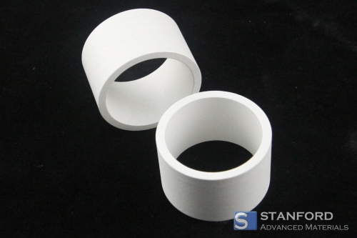
A typical example of an insulating wafer is a mica wafer. Mica is a general term for layered silicate minerals, which are insulating, transparent, heat-resistant, corrosion-resistant, easy to be peeled and elastic, etc. They are widely used in electric motors, electrical appliances, electronics, radio, and household appliances, and play an important role in the national economy and national defense construction. Although there are many kinds of natural mica, the main one used in industry is white mica, followed by gold mica.
Since synthetic mica has excellent characteristics of purity, transparency, high-temperature resistance, corrosion resistance, and electrical insulation, synthetic mica single crystal sheet can be used for:
① insulating frame in various vacuum devices, such as gas pedal, ionization chamber, magnetron, and electron tube;
② window material, such as microwave tube output window, high-temperature furnace observation window, and acid and alkali resistant window;
③ high-pressure boiler water level meter in thermal power plant;
④ high-temperature resistant capacitor, platinum wire Surface thermometer skeleton, etc.
Conclusion
Stanford Advanced Materials produces functional crystal materials for many application devices. Functional crystal materials mainly include magneto-optical crystals TGG terbium gallium garnet, TSAG; piezoelectric crystals LT (LiTaO3) lithium tantalate, LN (LiNbO3) lithium nioate, LGS lanthanum gallium silicate; scintillation crystals Ce: LUAG, Ce: GAGG; laser crystal Nd: YAG and single crystal epitaxial substrate crystals GGG, SGGG, lanthanum Aluminate LaAlO3, etc.
Crystal materials are widely used in the devices such as electric and optical adjustment Q switches, optical isolators, optical Rotators, etc. Optical isolators including Faraday free space isolators and fiber isolators vary from wavelength 450nm to 1100nm.