Silicon Carbide vs. Silicon: A Comparative Study of Semiconductors in High-Temperature Applications
1 Introduction
With the wide application of semiconductors in various aspects of production and life, the performance requirements for semiconductor materials in different use scenarios are becoming increasingly diverse. In many application environments, semiconductor materials must work at high temperatures, which demands high thermal stability, electrical stability, and power density of semiconductor materials. Under such requirements, Silicon Carbide (SiC) and Silicon (Si) wafers have received attention as semiconductor materials with stable structure and properties and good thermal stability. The diamond structure of these two atomic crystals makes them extremely thermally stable, and they can take on more semiconductor functions in high-temperature environments. In this article, we will analyze the differences in performance and reasons for their performance in high-temperature semiconductor application scenarios from the perspective of crystal structure and physicochemical properties, and provide references for your choices in combination with the preparation process and cost.
2 Crystal Structure and Properties of Silicon Carbide and Silicon Wafer
2.1 Crystal Structure and Properties of Silicon Carbide
According to the crystal structure, silicon carbide can be divided into hexagonal α-silicon carbide and cubic β-silicon carbide. α-silicon carbide (α-SiC) is the most common polycrystalline type, and according to the arrangement of the atoms, it is divided into 4H-SiC and 6H-SiC, and in the 4H-SiC crystal structure, the silicon atoms and the carbon atoms are arranged in alternating layers, which forms the hexagonal crystal lattice structure; whereas in the 6H-SiC, it forms the alternating hexagonal and tetragonal crystal lattice structure. Figure 1 illustrates the atomic arrangement of these two crystal structures.
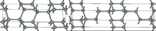
Fig.1 Crystal Structure of 4H-SiC(left) and 6H-SiC(right)
For α-SiC, some of the properties of 4H-SiC and 6H-SiC are slightly different due to minor differences in their lattice structures. 4H-SiC has a large lattice mismatch tolerance, which characterizes the ability of the crystal to maintain a certain degree of stability and crystalline quality even when there is an imperfect match between the atomic arrangements in the lattice and is an important parameter for describing the plasticity and stability of the crystalline material under the action of stress. It is an important parameter to describe the plasticity and stability of crystalline materials under stress. The combination of larger lattice mismatch tolerance with higher breakdown field strength and better electrical conductivity results in better stability and reliability of 4H-SiC devices, which perform well in high-power electronics and optoelectronics. In contrast, 6H-SiC has higher electron mobility and lower electron capture cross-section, which gives 6H-SiC better carrier transport properties, including mobility and lifetime.
The β-silicon carbide (β-SiC) can be represented as 3C-SiC according to the atomic arrangement, where each silicon atom is surrounded by four carbon atoms and four neighboring silicon atoms in the cubic lattice structure. Figure 2 shows the structure of its atomic arrangement.
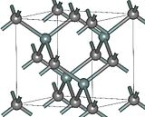
Fig.2 Crystal Structure of 3C-SiC
Compared to β-SiC, α-SiCs offer better cost-effectiveness and device reliability because their crystal structures have better stability, lower impurity concentrations, and lower defect densities, which allow them to operate at high temperatures, high power, and high voltage conditions. As for 3C-SiC, its crystal structure allows it to have the highest theoretical electron velocity, but it is susceptible to impurities, resulting in impurity corrosion traces. 3C-SiC has a high electron mobility and electron saturation drift rate, as well as low impurity concentration and leakage currents, which allows it to be used in high-power electronics, RF devices, etc., but due to the difference in its crystal lattice structure and silicon substrate materials and therefore not suitable for integrated circuit fabrication. Different crystal structures of SiC specific physical and chemical properties and crystal structure of the relevant parameters can be seen in Table 1.
Table 1 Properties of SiC crystals with different crystal structures
|
Type |
3C |
4H |
6H |
|
Crystal Structure |
Sphalerite-Type Structure (Cubic Crystal System) |
Hexagonal Crystal System |
Hexagonal Crystal System |
|
Space Group |
T2d-F43m |
C46v-P63mc |
C46v-P63mc |
|
Pearson Symbol |
cF8 |
hP8 |
hP12 |
|
Cell Parameters(Å) |
4.3596 |
3.0730; 10.053 |
3.0810; 15.12 |
|
Density(G/Cm3) |
3.21 |
3.21 |
3.21 |
|
Bandgap Reference(eV) |
2.36 |
3.23 |
3.05 |
|
Bulk Modulus(GPa) |
250 |
220 |
220 |
|
Thermal Conductivity [W/(M·K)] |
360 |
370 |
490 |
2.2 Crystal Structure and Properties of Silicon
Silicon crystals have a typical diamond structure, with silicon atoms arranged equidistantly to form a cubic lattice, and each silicon atom connected to the four surrounding silicon atoms through covalent bonds to form an extremely stable ortho-tetrahedral structure, which gives silicon monomers a high melting point (1414°C) and thermal stability. Figure 3 is a schematic representation of the structure of a silicon crystal.
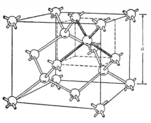
Fig.3 Crystal Structure of Si
Each silicon atom in a silicon crystal is connected to four surrounding silicon atoms by covalent bonds, forming a stable crystal structure. This makes silicon chemically and thermally stable, with a melting point of about 1414 degrees Celsius. Silicon also has a high thermal conductivity of about 1.5 to 1.7 watts per meter-kelvin (W/m-K), which makes it important for heat dissipation and thermal management applications. Silicon is an indirect bandgap semiconductor with a bandgap width of about 1.1 electron volts (eV). At room temperature, silicon behaves as an insulator, but when excited (e.g., by an increase in temperature or the application of an electric field), electrons can jump into the conduction band, making it a semiconductor. In pure silicon crystals, the concentration of electrons and holes is very low, so it behaves as an insulator. However, by doping or applying an electric field, additional free carriers can be introduced, causing silicon to exhibit the conductivity of a semiconductor or conductor.
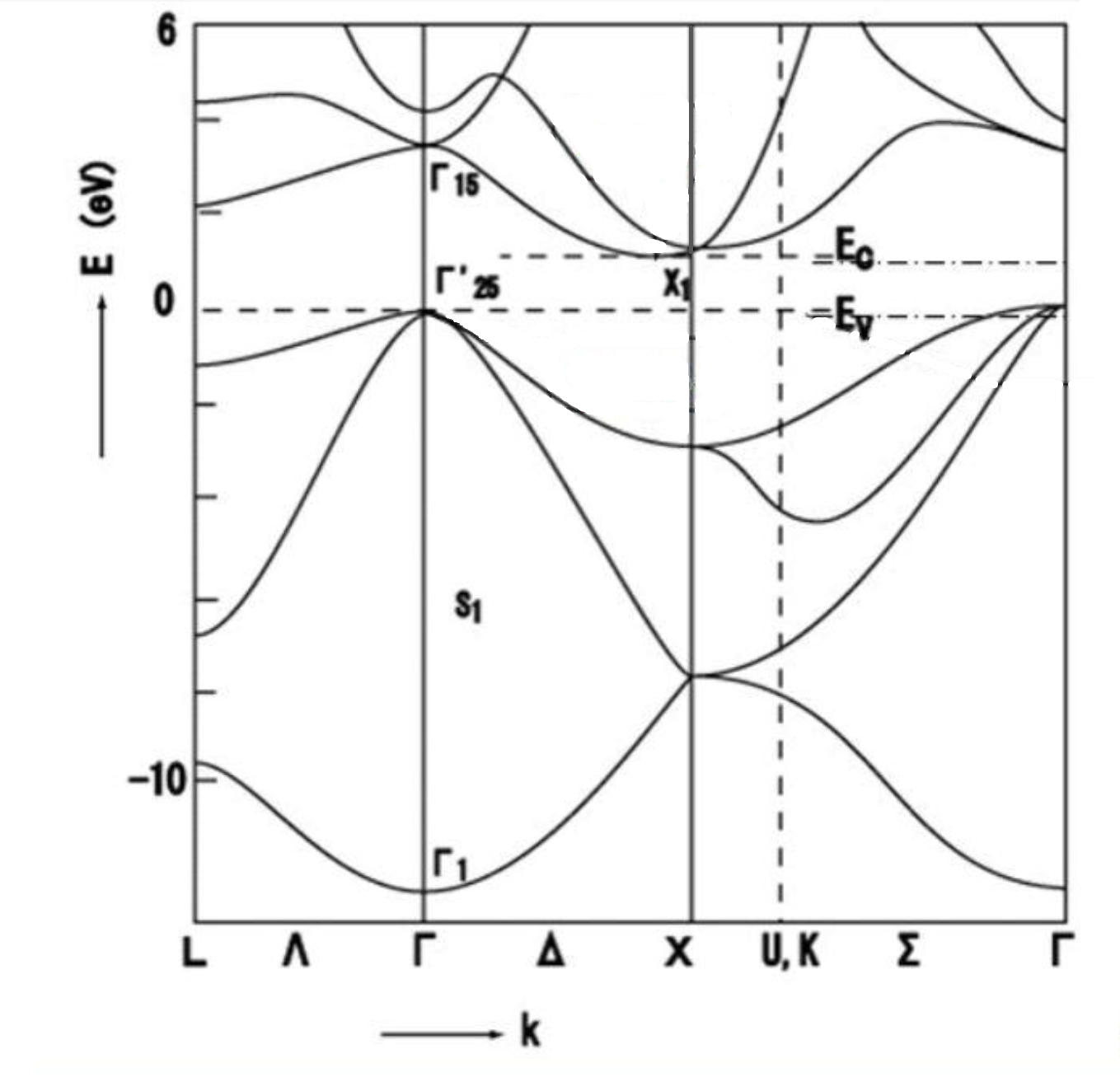
Fig.4 Diagram of the Energy Band Structure of a Silicon Crystal
3 How SiC and Si Are Better Than Other Semiconductor Materials
3.1 Challenges to Semiconductor Materials in High-Temperature Environments
At high temperatures, materials are susceptible to thermal stress and thermal expansion, leading to disruption of the crystal structure and degradation of properties. For semiconductor materials, especially those such as silicon, thermal stability is critical. The crystal structure not only affects the performance index of the device but also may have a direct impact on the operation and safety of the whole process. At the same time, the electrical properties of semiconductor materials are prone to change in high-temperature environments, for example, conductivity, carrier concentration, etc. may be affected by the temperature and change, which may lead to a decline in the performance of electronic devices or failure. In addition, semiconductor materials in high-temperature environments are prone to chemical reactions with oxygen, water vapor, etc. in the surrounding environment, resulting in oxidation of the surface of the material, corrosion, or diffusion of impurities in the material, and other phenomena, affecting the stability and life of the device. The heat generated inside the device working in a high-temperature environment may also cause the temperature to rise again, thus affecting the performance and stability of the device. Therefore, good thermal conduction and heat dissipation systems are critical for semiconductor devices in high-temperature environments.
3.2 Advantages and Disadvantages of Silicon Carbide and Silicon
3.2.1 Thermal Properties
Si has a melting point of about 1414 degrees Celsius and SiC has a melting point of about 2700 degrees Celsius. The thermal conductivity of silicon is about 1.5-1.7 watts per meter-kelvin (W/m-K). SiC has a higher thermal conductivity, typically between 3 and 4.9 watts per meter-kelvin (W/m-K), depending on temperature and crystal structure. As shown in Figure 5, the thermal conductivity of silicon carbide is three times higher than that of silicon. From a comprehensive view of the ability to withstand high-temperature environments, SiC can withstand higher temperatures than Si and has more excellent heat dissipation performance, which can be prioritized in the use of extremely high-temperature requirements.
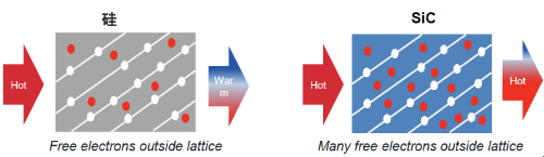
Fig.5 Silicon Carbide Has 3 Times Higher Thermal Conductivity Than Silicon
3.2.2 Photoelectric Properties
SiC is a wide-band semiconductor with a bandgap width of 2.2 to 3.3 electron volts (eV) Si is a narrow-band semiconductor with a smaller bandgap width of about 1.1 electron volts (eV). The bandgap width determines the conductive properties of the material. Materials with a small bandgap usually behave as good conductors or semiconductors because electrons can jump into the conduction band with relative ease and participate in the conductive behavior. Materials with larger bandgaps, on the other hand, usually behave as insulators because electrons require higher energies to jump into the conduction band, resulting in materials with few free carriers at room temperature. The bandgap width also determines the optical properties of the material such as absorption, emission, and transmission of light. Materials with smaller bandgaps usually exhibit good light absorption properties because they can absorb more photons. Materials with larger bandgaps, on the other hand, are usually transparent or translucent because they can only absorb photons with energies greater than the bandgap width. These different property performances also determine that SiC and Si are applied in different usage scenarios.
3.2.3 Mechanical Properties and Chemical Stability
The Mohs hardness of SiC is about 9-9.5, which is close to the hardness of diamond, while the Mohs hardness of Si is about 7, which is slightly lower than that of SiC. SiC's high hardness gives it good abrasion and scratch resistance, making it suitable for use in the fabrication of devices that require abrasion resistance. At the same time, the strength of SiC is usually higher than that of Si. SiC has excellent flexural and tensile strengths and can withstand greater stresses without deformation or rupture. SiC has good chemical stability at room temperature and is not easily attacked by acids, alkalis, and solvents, while Si is attacked by some strong oxidizing agents and strong acids.
4 Different Application Scenarios for Silicon Carbide and Silicon
Considering the distinct properties of SiC and Si arising from their crystal structures, it's evident how their applications are tailored to their strengths.
SiC boasts exceptional thermal stability and resistance to high temperatures, making it ideal for crafting electronic devices that operate under extreme heat conditions. Applications include power devices, RF devices, and more. Its robust performance in high-temperature environments opens up possibilities for meeting demands in sectors like power electronics, RF communications, and automotive electronics. Furthermore, SiC's wider bandgap width translates to higher breakdown voltages and lower on-resistance, making it particularly suited for manufacturing high-power devices such as power MOSFETs and diodes.
On the other hand, Si stands out as one of the most prevalent semiconductor materials, finding extensive use in conventional electronic devices like transistors, integrated circuits, and solar cells. It serves as a cornerstone material in microelectronics, benefiting from mature preparation technologies and processing methods that enable high levels of integration and miniaturization. Si's versatility extends to optoelectronic applications such as LEDs, lasers, photodetectors, and solar cells, leveraging its excellent photovoltaic properties and photoelectric conversion efficiency.
5 Conclusion
Compared with silicon, silicon carbide tends to have a wider range of applications in higher temperature scenarios, but due to its preparation process and the purity of the finished product obtained, silicon wafers are still the more commonly used choice in cases where the temperature environment requirements are relatively low. Stanford Advanced Materials provides high-quality Silicon Carbide Wafers and Silicon Wafers for your various utilizations.
Related Reading:
Heating Elements: Molybdenum Disilicide vs Silicon Carbide
Case Study: Silicon Carbide Plates for Advanced Armor Solutions
The Breakthrough of Silicon Carbide Substrate in LED Industry
Reference:
[1]Fenglin G ,Chen S ,Xiufang C , et al. Shape modulation due to sub-surface damage difference on N-type 4H–SiC wafer during lapping and polishing[J]. Materials Science in Semiconductor Processing,2022,152.